
Context
Earlier this year, I embarked on the exciting journey of assembling a pristine purple silkscreened Amiga 500++. While I must admit that clear cases aren’t typically my go-to choice, I firmly believe they are a necessity when you’ve poured meticulous time and care into crafting something extraordinary. If it looks different or possesses that special charm, then it unequivocally deserves to be showcased! I housed my 500++ into a transparent case to show off its glory and all the attention to detail for example the matching purple silkscreened keyboard PCB.
Now, here’s where the plot thickens. You see, I happen to possess one of the most remarkable expansions ever conceived for the 500 – the ACA500 by the ingenious Jens. However, that contraption finds its home in my other Amiga machines. For this particular 500++, my vision was one of a self contained microcomputer, where every enhancement resides within.
In my quest for suitable internal expansions and on April 16th, 2023, when I stumbled upon jbilander’s Spitfire 500. It’s a marvel of simplicity, impeccably designed to amplify the 500’s capabilities. Notably, it retains the Amiga 68000 CPU with the power to sprint at a brisk 14MHz using a double clock speed, a generous dose of 8MB fast RAM, and offers an IDE interface to boot. I reached out to Levoman and shared my intent to embark on this Spitfire 500 adventure. In response, he generously shared links to an alternative KiCad version available in kit form. However, my discerning eye identified two crucial deal-breakers: Firstly, it lacked the resplendent purple hue I so adore, and secondly, it lacked the coveted IDE functionality.
We also explored Stephen Leary’s TF536, an enticing prospect in its own right. however securing a genuine purple PCB for this endeavor proved to be an impossible excercise.
Ordering
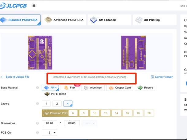
So, as time passed, other projects started to take precedence (maybe I’ll share some of those stories sometime). Eventually, I downloaded the gerber files for the PCBs from the GitHub repository. Curiosity got the better of me, and I decided to check out the prices. I tried the usual suspects – JLCPCB and PCBWAY, but in the end, I settled for JLCPCB. The board in question is a 4-layer marvel, and I opted for the HASL finish to keep everything consistent. Levoman’s sage advice always resonates – unless you have any gold fingers then there is really no point in the extra expense, especially when it’s going to be soldered in any case. I placed an order for QTY 5 V1b boards on April 20, 2023.
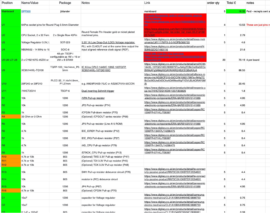
I created an Online Bill of Materials (BOM) and commenced the tracking down the necessary components from various suppliers. The screenshot I’ve provided below represents just a fraction of the complete BOM and may not be entirely legible. Nonetheless, it should offer you a glimpse into the sheer magnitude of effort required to embark on a project of this nature. I managed to secure the U10 ICs from Levoman, pre-programmed and all – a nod to his mantra of “Salvage, let’s save the planet, one chip at a time.”
In the end, I had all the items on the BOM ordered by April 26, 2023 – 90% of it from Digikey
Delivery
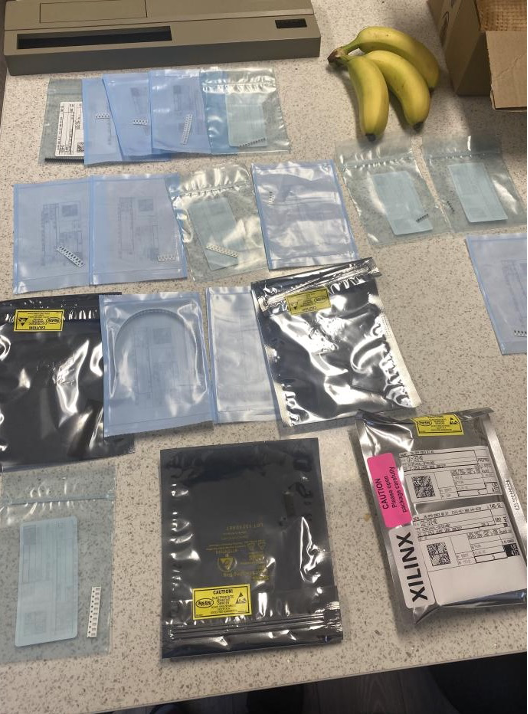
Fast forward to April 30th, and there it was – the BOM had miraculously arrived! Well, almost all of it, with the exception of the RAM. What you see are genuine components sourced from DigiKey and all low tolerance parts to give you that warm fluffy feeling.
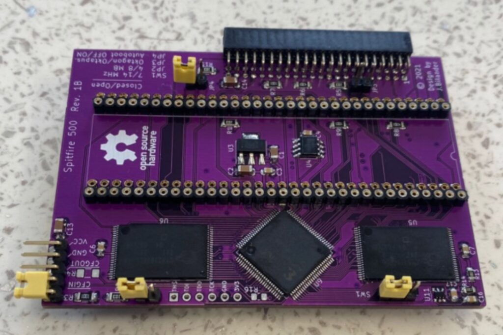
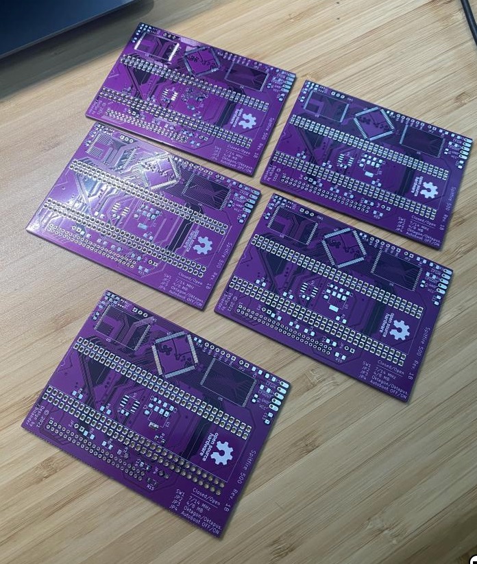
On the 3rd of May, the eagerly awaited pruple PCBs made their grand entrance, marking a significant milestone in this project’s progress – They look gorgeous dont they?
Assembly
My initial plan was to kick off the testing phase of the boards, and these were the steps I had in mind
- Begin by soldering on the CPLD.
- Grab a USB cable and re-terminate one end to fit a DuPont connector.
- Using this cable, I supply 5V to VCC and power-up a single Spitfire.
- Then, probe and prod with a multimeter to ensure that the voltage and ground were in their rightful places.
However, due to the delayed arrival of the RAM, I hesitated to proceed with these steps. Eventually, on the 16th of May, 2023, the RAM made its much-anticipated appearance. This wasn’t too much of a big deal as I had a backlog of other projects to tackle in any case.
As previously mentioned, the initial step involved mounting the CPLD and assessing the voltage levels. Upon close inspection, the pads for the IC appeared somewhat questionable, and we agreed that a thorough pad cleanup using flux and braid should suffice to address the issue.
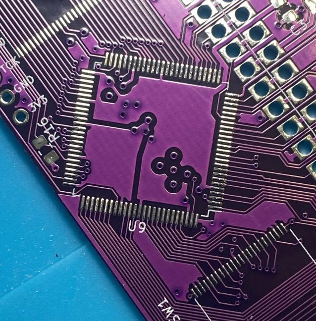
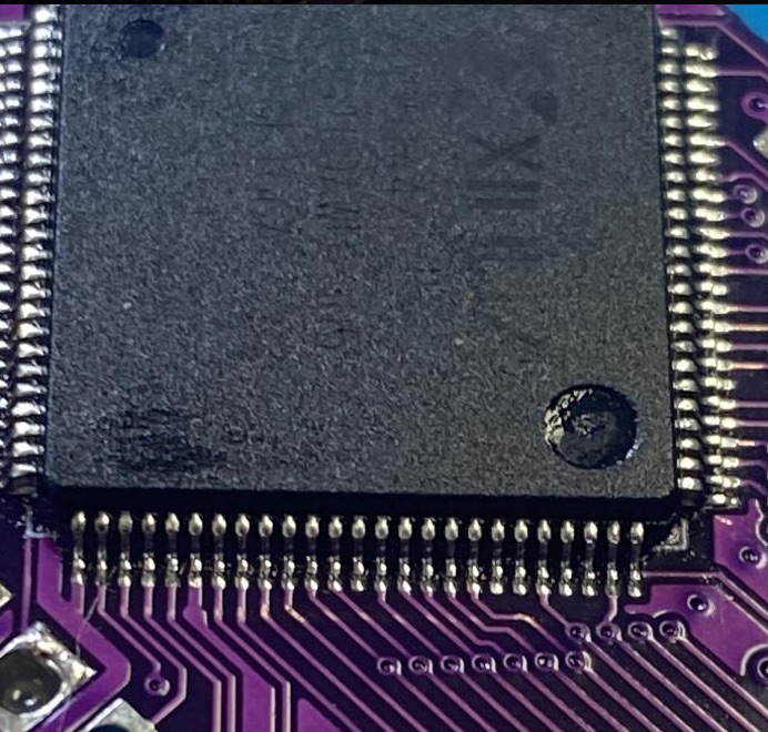
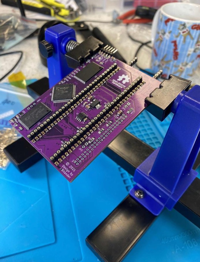
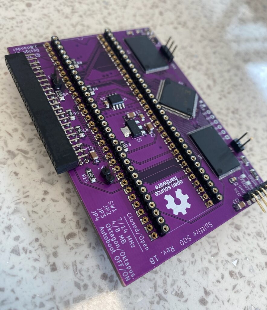
With the solder pads cleaned up, the next critical step was to mount the CPLD. Ensuring correct orientation was absolutely vital. I meticulously observed the IC, noting that three corners featured a simple 90-degree shape, while one corner bore a distinctive “Z” marking, designating it as pin one. To further safeguard my sanity and obtain a second opinion, I cross-referenced images from the GitHub repository and even reached out to Levoman for a peer review of my work. I was using a brand new soldering station so getting used to the tips and tools as well as using a smaller gauge solder was a quick steep learning curve with no margin of error.
Continuing in accordance with my previous steps, I proceeded to install the voltage regulator along with some capacitors. After ensuring everything was in place, I applied 5V power to the board and employed a multimeter to measure the voltages. As expected the reading showed a steady 3.3V!
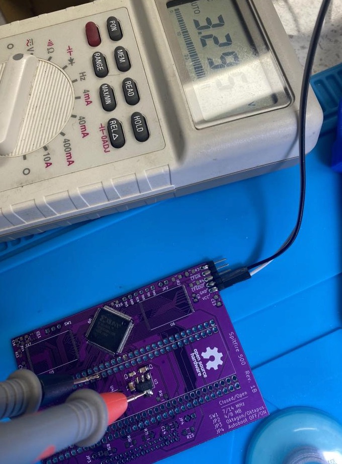
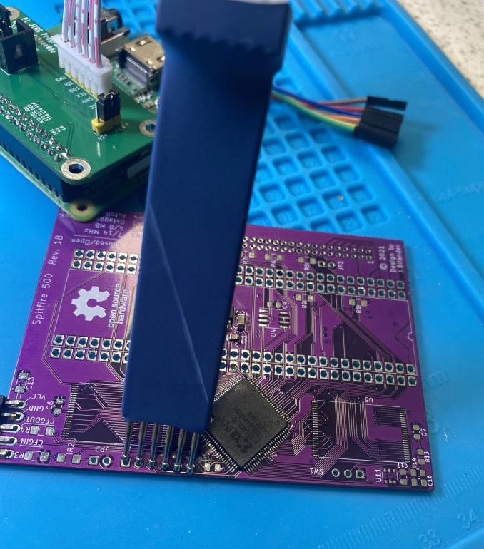
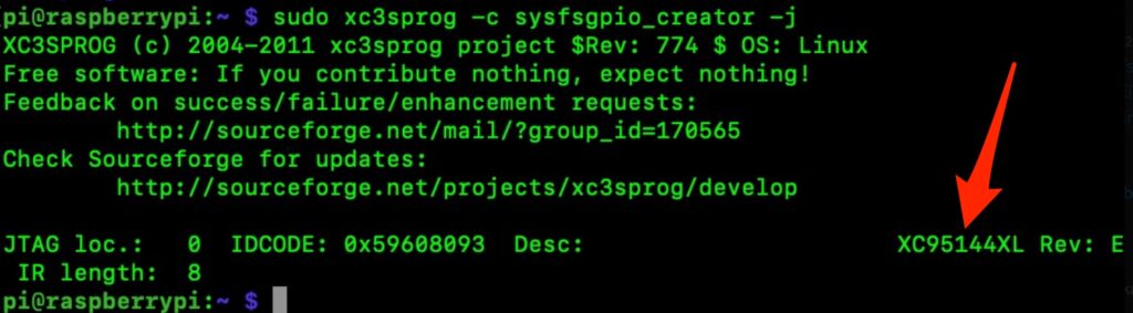
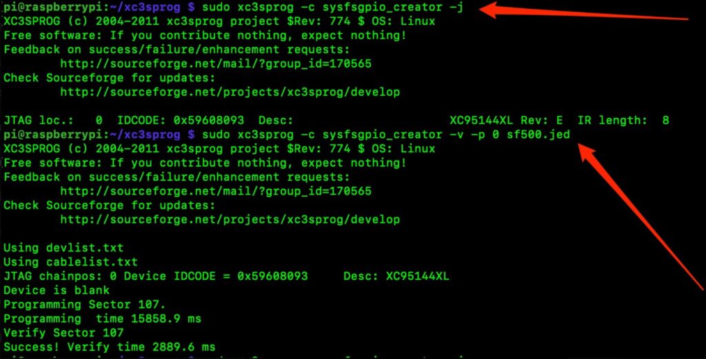
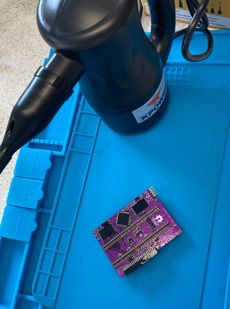
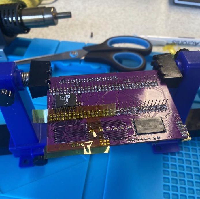
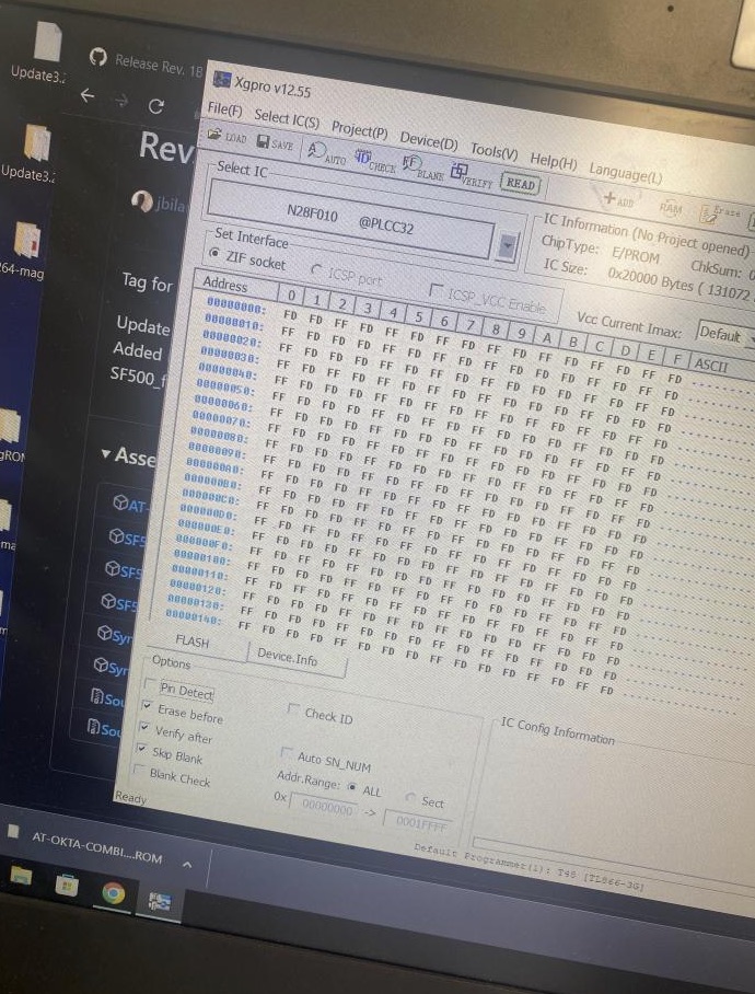
Moving forward, my objective was to establish communication with the CPLD through the JTAG header. I configured my Raspberry Pi with X3CPROG and used a Pogo probe, as depicted in the subsequent two images. The green-on-black display represents a screenshot of my session with the Pi, which was dedicated to interacting with and testing the CPLD. As you can see I was able to query the CPLD and get it to spit its version back at me – Great so far !
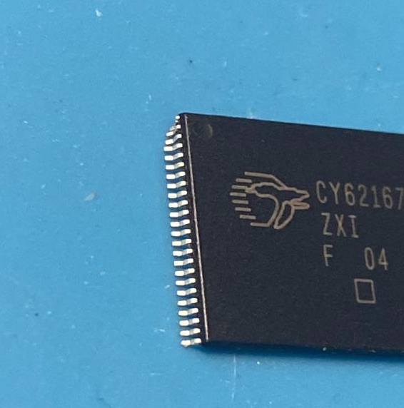
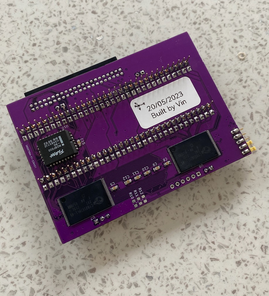
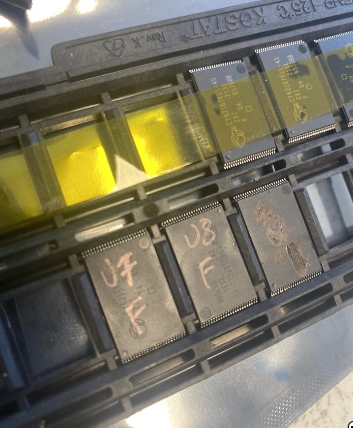
My next task on the agenda was to install the SRAM. Unfortunately, I encountered a mishap and dropped one of the SRAM chips. Regrettably, I hadn’t ordered any spares, which left me in a bit of a predicament. However, I had sufficient parts for assembling the other boards. So, I resorted to a classic “borrow from Peter to pay Paul” scenario to keep the project moving forward.
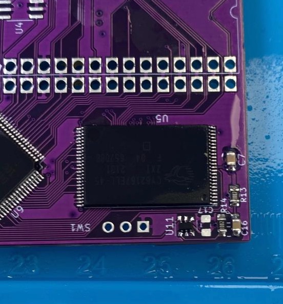
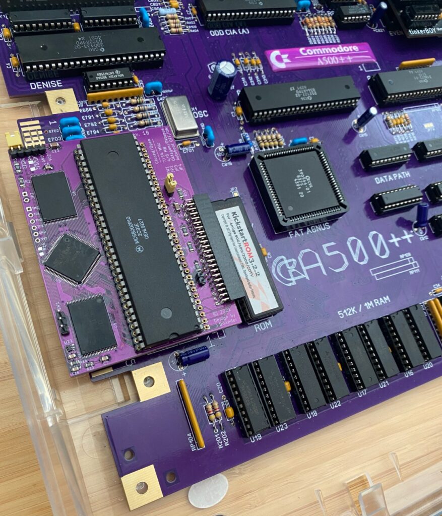
Paying attention to the orientation of the RAM was crucial, and the silkscreen’s long white line extending to pin one served as a helpful guide. Following this, I moved on to the ROM (U10) installation. These were JLEG, a bit tricky for those lacking experience, particularly when attempting to achieve a well-formed solder heel. There are various techniques available, but ultimately, I recommend sticking with the method you’re most comfortable with. After soldering, it’s always a good practice to verify continuity to ensure a solid connection.
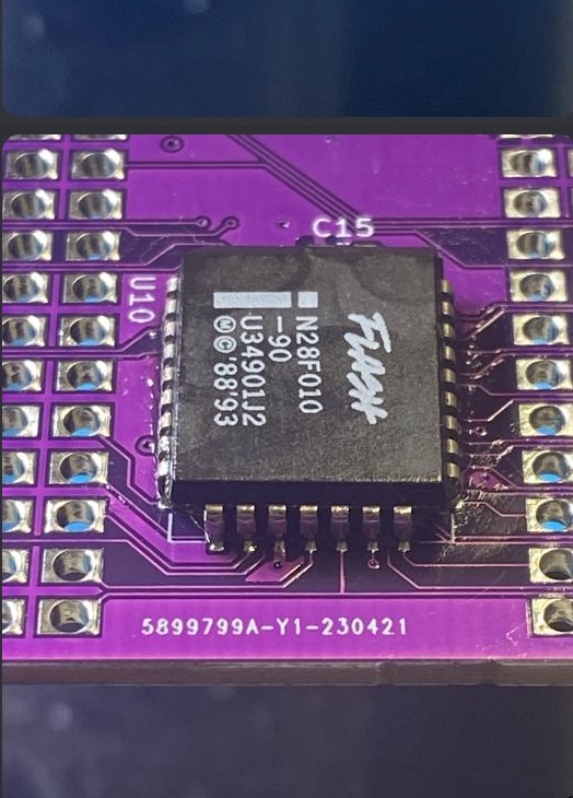
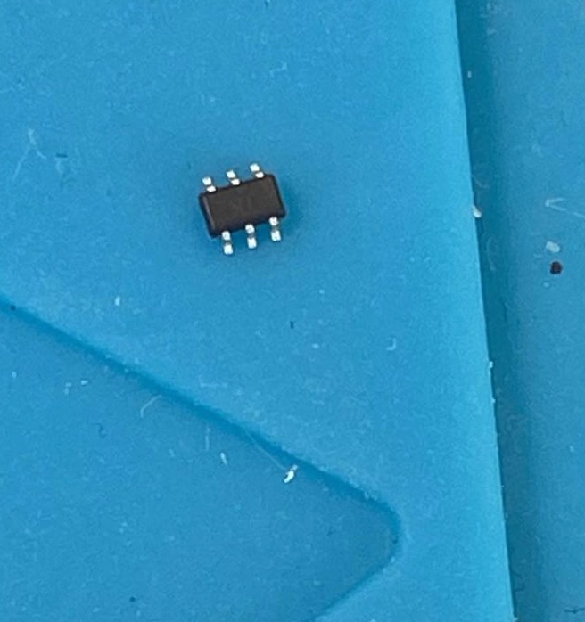
Continuing with the assembly process, the next component in line was all the SMD caps and resistors and the U11. However, I encountered an issue where this tiny component didn’t align perfectly with the pads. Despite the alignment hiccup, I decided to go ahead with the installation and then sought guidance from Levoman. He clarified that the alignment discrepancy was acceptable, but the root cause of the issue was that this component should have been the TSOP version (74HCT2G14GV,125) rather than the TSSOP version (GW)
Navigating the maze of IC orientations proved to be quite perplexing. Levoman, equally shared my frustration, wondering aloud why manufacturers insist on making it so confusing. It seemed that different markings for pin 1 were employed on various outlines, not to mention the varying sizes of chips and the involvement of multiple manufacturers. This is a puzzling situation pondering about the supposed standards that were supposed to simplify matters.
Next was to start soldering on all the header pins and the IDE connector. The PCB holder I used proved helpful. You can see a mini jig by using header pins on the bottom also.
Finally, the moment of truth – power up time
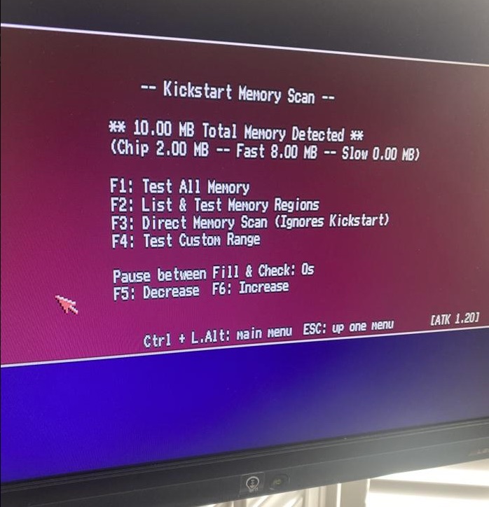
Memory test with Amiga Test Kit 1.20 (ATK)
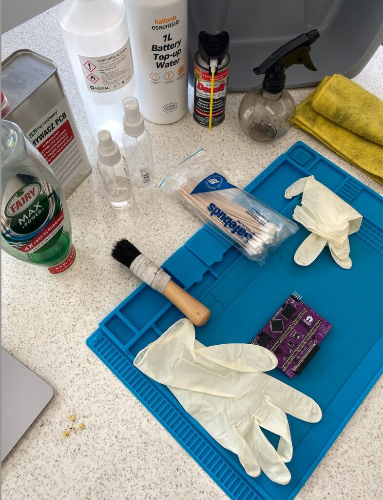
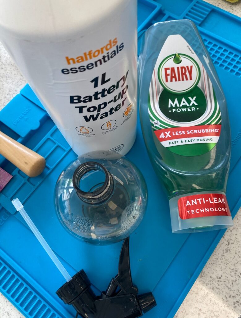
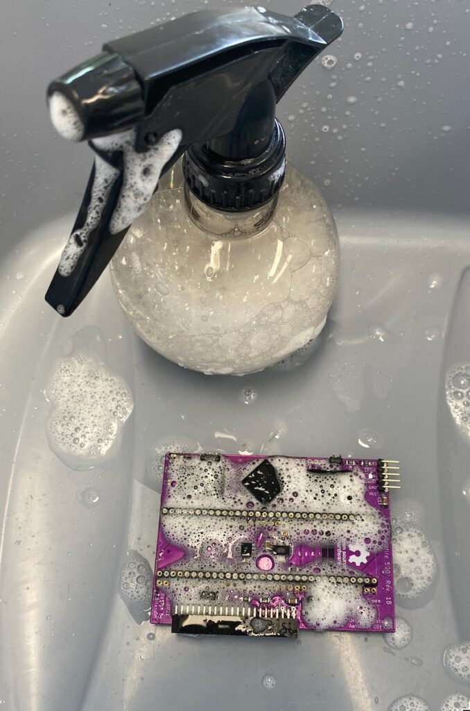
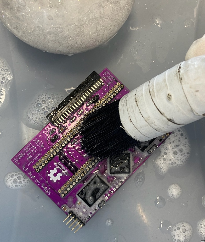
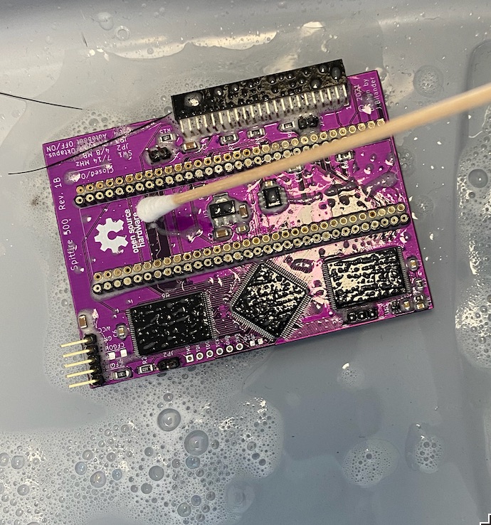
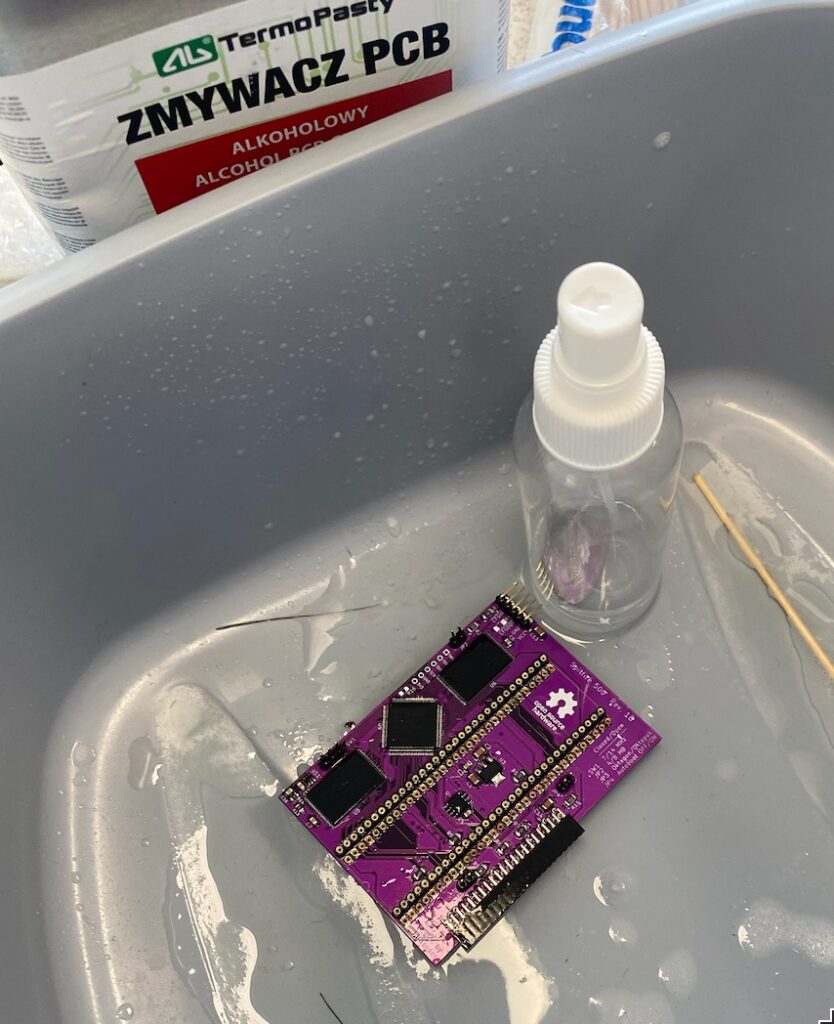
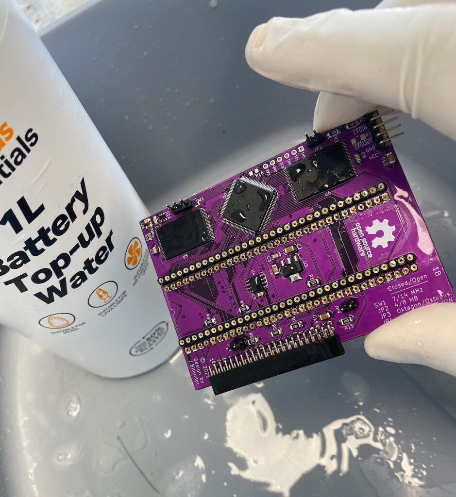
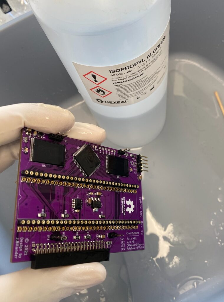
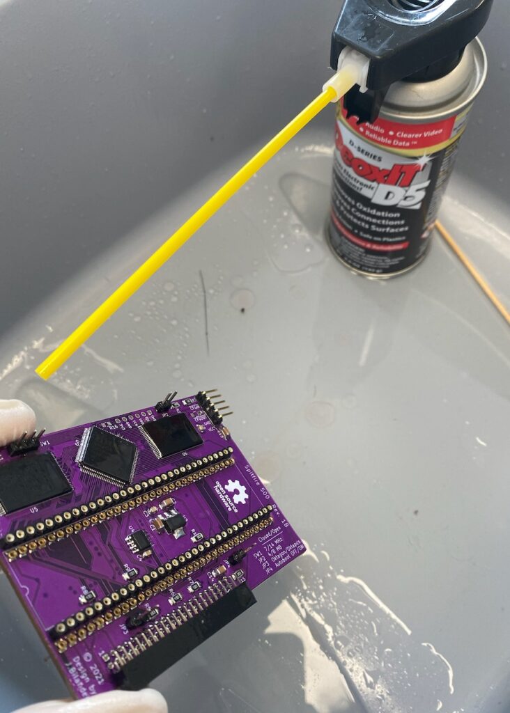
Board Cleanup !
Before the assembled boards can be marked of as completed they do need cleaning up of any flux residue, here is how I did this.
Lessons Learnt
These lessons learned should prove invaluable for anyone embarking on similar projects.
- Diversify Component Sources: If you’re open to purchasing components from multiple vendors, you can often reduce costs. Not every component requires low tolerance parts from Japan.
- Peer Review Your BOM: Mistakes can easily slip into your Bill of Materials (BOM), so having someone review it can catch errors. Pay particular attention to component variants, such as TSOP vs. TSSOP.
- Order Spare Components: Always order extras. If you lose, damage, or encounter a faulty component, not having spares can cause significant delays in your project.
- Pin 1 Markings: When soldering, deciphering the pin 1 markings can be challenging. Consult reference pictures and, if possible, print them out in color for clarity.
- Take Your Time with Unfamiliar Components: If you’re dealing with a component you haven’t soldered before, go slowly. There are plenty of helpful guides on platforms like YouTube. If in doubt, seek advice from us.
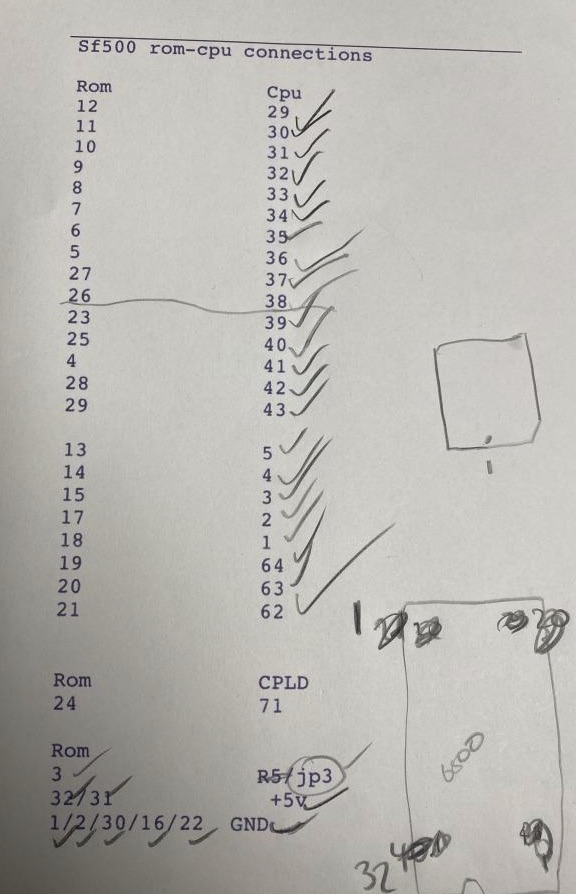
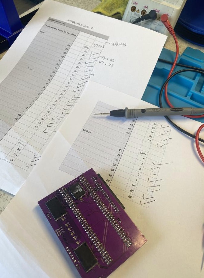
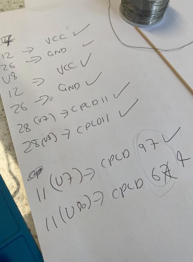
- Troubleshooting Challenges: In the other SF500 board assemblies, I encountered issues like faulty RAM, a missed solder leg on the PLL, and a CPU not handling the 14MHz. Troubleshooting can be daunting and super stressful – you may feel like giving up. Begin by taking a break! Then start reviewing any notes provided by the designer, meticulously check soldering against the schematics, and conduct continuity tests on all connections. Examining components under magnification or using high-resolution images taken with your mobile and viewed on your PC monitor can be extremely helpful if you lack a microscope.
Below are some images/text from the troubleshooting process…
Finally….
This neat little package turned out to be precisely what the doctor ordered. It provided a subtle speed boost, making the machine noticeably snappier. Moreover, having the ability to incorporate an HDD and boot directly into Workbench streamlined the user experience. The extra RAM also opened the door to running WHDLOAD, allowing for game launches. All in all, it was a transformative addition to the setup Highly recommended !
I agree , A good addition to the A500 . It does not boast the speed increases of an ‘030 or ‘060 accelerator , but it does help with the extra ram and internal drive option .
Not recommended as a first time build , but if you think you can do the SMD soldering without too much issue , a very rewarding one .
Will you consider making some for sale?
It might be worth asking on AmiBay .
https://www.amibay.com/forum
It is free to sign up and there is help and items for sale for all sorts of computers not just the AMIGA .
Very nice write-up! Thanks for taking the time writing it, and I’m very glad you seem to like the SF500. Nice job! Nice soldering! Best Regards, Jorgen
I’m not sure why but this site is loading extremely
slow for me. Is anyone else having this issue or is it a problem on my end?
I’ll check back later and see if the problem still exists.
Hello Vin,
Can you share your Online Bill of Materials? with link to the parts?
Thanks