This is a very common question asked by any new comer to the hobbyist electronics arena ‘ Where is pin 1 ? ‘ .
I will endeavour to give the value of my experience in the field , and help you to identify pin 1 on any chip that I can .
We have to start with pictures , how can you identify it if you have not seen it ?
Through Hole devices
So called because they have legs that go through a hole in the PCB , or can be mounted in DIP ( Dual In-line Package ) or SIP ( Single In-line Package ) sockets .
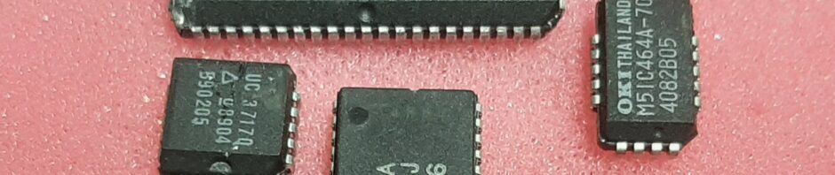
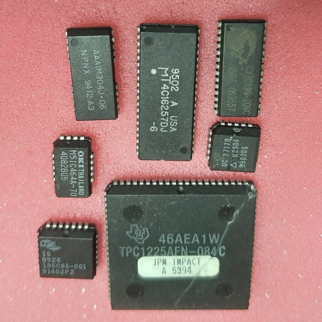
Starting with DIP chips . In the correct orientation pin 1 is always the top left pin .
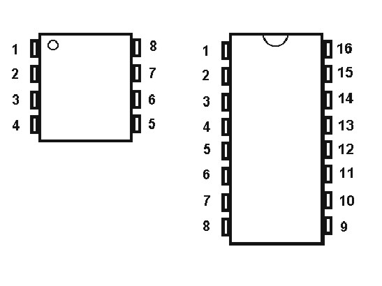
If you have not noticed there are two different variations of showing which end pin one is on , On the 8 pin chip there is a dot next to pin one , and on the 16 pin chip the notch in the middle denotes the pin one end .
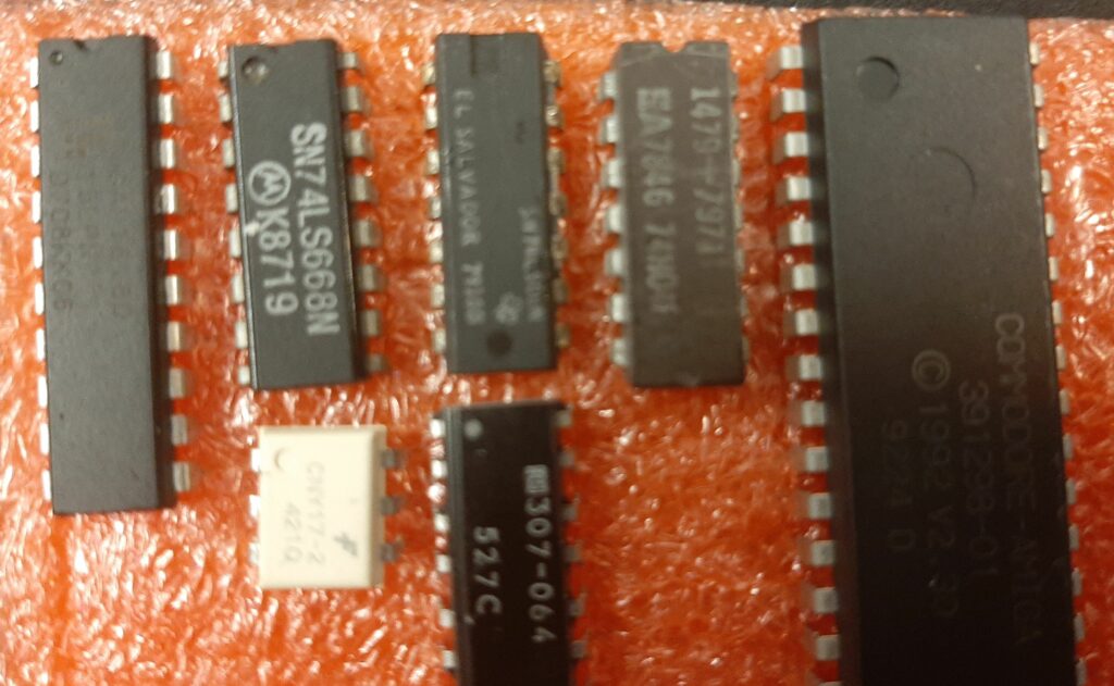
Having gone through the vast array of through hole DIP chips I have , these are the different pin one markers that I could come up with .
SIP chips are even easier .
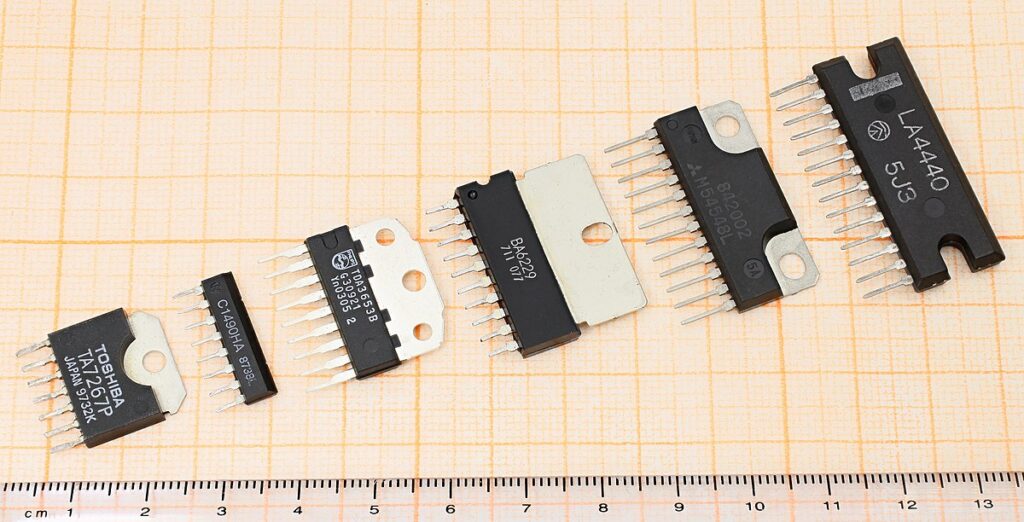
Basically with the writing ( IC identification number ) facing you and the pins at the bottom , pin 1 is the bottom left .
ZIP chips identify in exactly the same way as SIP chips , but the legs are staggered into two rows . They are still numbered from left to right exactly the same as SIP chips .

J-lead packages
So called because the leg forms a ‘J’ by going under the edge of the chip also known as PLCC IC’s .
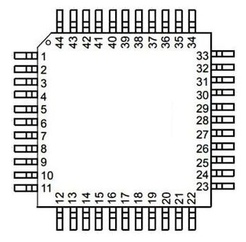
J-lead chips become a little more difficult , because now we get square chips and different leg configurations .
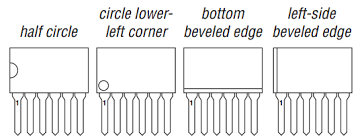
On the square ones pin 1 is directly below the dot and pin 1 side is marked by a cut off corner on the top left of the chip , and the others tend to follow the through hole method of pin 1 marking . The square one’s also tend to have a beveled edge on the pin 1 side and the DIP ones on the pin 1 end , but not always .
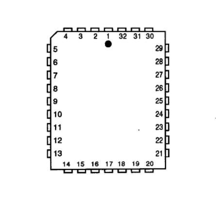
The pin numbering goes from pin 1 around to the left and all the way around the chip to finish by pin 1 , no matter how many pins the chip has .
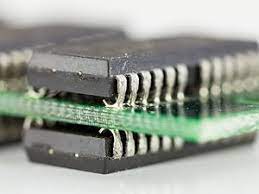
Surface Mount Devices ( SMD for short )
This is where things get really difficult ! Not just because of the multitude of chip designs , but also due to the very small size of some of the components , and the size of the marker .
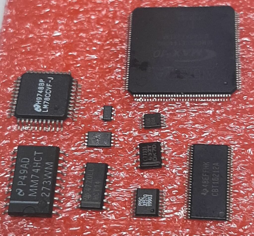
We now have lines marking pin 1 end , as well as the traditional dots and semi-circle marks . On the square chips , pin 1 has moved to the top left corner and pin one is on the top of the left hand side of the chip . See how small the 5 pin device is ! The pitch ( gap between them ) of the pins gets smaller as well with the thickness and size of the package .
NEXT : Pin 1 on the PCB .
I have an Issue 2 pack - so if it works I'll send the details and you will have a…